

Overview
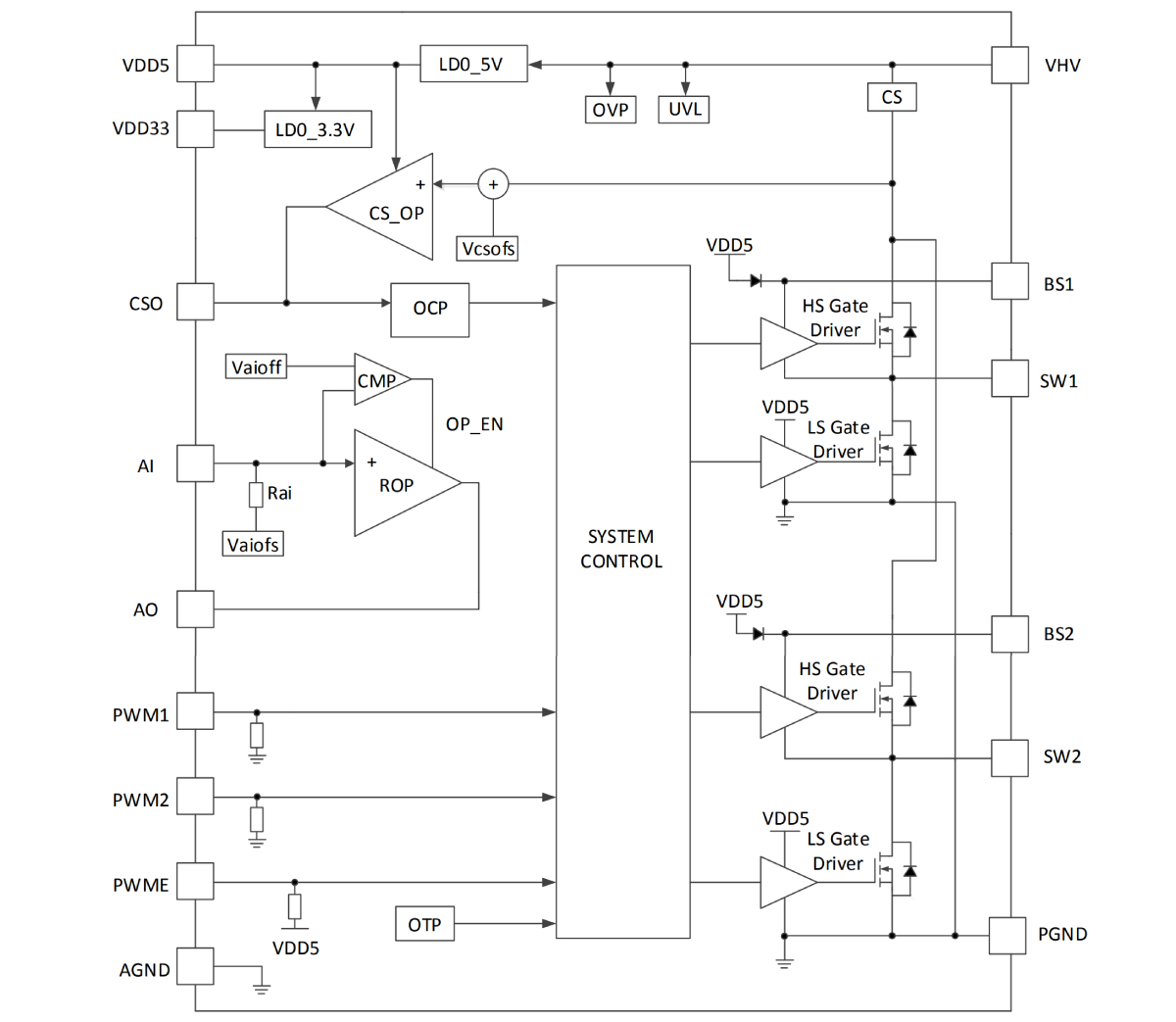
CH275 is a full-bridge power chip with four built-in power switching tubes and current sampling module and wireless charging feedback signal amplifier module. The chip integrates over-current protection, over-temperature protection, over-voltage protection, under-voltage lockout and other modules, supports FOD foreign object detection, and has a built-in LDO regulator to provide 5V or 3.3V power supply for the MCU, with streamlined peripheral devices, which can be used for the transmitter side of the wireless charging or motor drive.
The following is the internal block diagram of CH275 for reference only.
Features
- Built-in 4 N-MOSFET power switching tubes, typical 20mΩ on-resistance.
- Rated 2A continuous on-state current, supports 5A peak current.
- Built-in low dropout bootstrap diode, peripheral only need capacitor.
- Built-in Current-Sense current sampling and amplification circuit, supports FOD foreign object detection.
- Built-in wireless charging feedback signal amplifier module ROP, supports MCU signal demodulation.
- Built-in power tube over-current protection module OCP.
- Built-in chip over-temperature protection module OTP.
- Built-in power supply over-voltage protection module OVP and power supply under-voltage lockout module UVL.
- Built-in LDO low dropout regulator, generates 5V and 3.3V for MCU simple power supply.
- PWM input control signal level compatible with 5V, 3.3V and 2.5V voltage MCU or FPGA.
- Integrated dead-time control, supports PWM up to 500KHz switching frequency.
- Support 5V, 9V, 12V, 15V, 20V and other power supply voltages, high energy conversion efficiency.
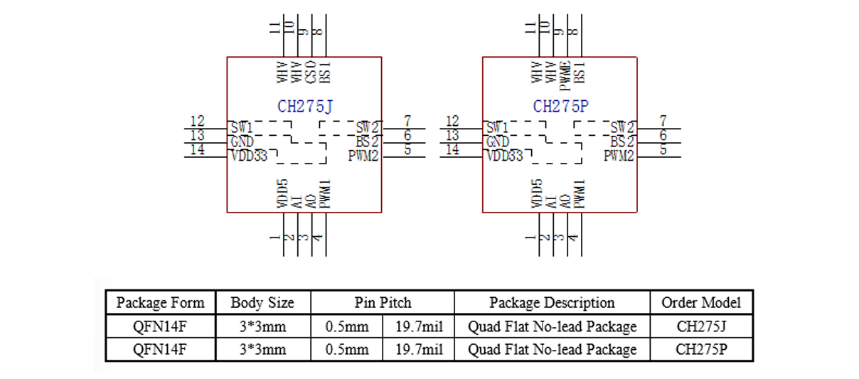
- Available in QFN14F and other packages.
Package